My work with the Immunogenetics Lab at the Johns Hopkins School of Medicine involves developing a microfluidics platform for homogeneous (single strand) HLA (human leukocyte anitgen) allele detection.
When people need an organ transplant, they have to find a matching donor. One of the methods used to check if two people are a match is sequence-based typing. This means that the DNA of those two individuals is compared to see if certain parts are the same. That part is the HLA, the major histocompatibility complex for humans (the stuff that controls your immune system). For each gene (part of our DNA) we have two alleles (different varieties). You get one from your mom and one from your dad.
When blood is drawn (the source of DNA for this lab), it contains both varieties. Usually, they are tested at the same time. This means that looking at the sequenced DNA is like looking at two words on top of each other like this APPLESORANGES. This is pretty hard to read! However, if I tell you that the names of two types of fruit are overlapping, you might be able to figure out what it says (APPLES and ORANGES). Similarly, by having some knowledge of common alleles we can usually figure out how to separate the information from a heterozygous (both at the same time) typing.
However, not every set of sequences is easy to separate out into the two components. For instance, if I put the work BACK on top of the word TALL, it could be incorrectly separated as BALL and TACK. Another case that is problematic is when someone has a sequence that has never been typed before. In this analogy it would be like saying separate out the two overlapping words, but one (or both) of them is a new word that you have never seen before. This is where I come in! I am working on a device that will take a sample from a person's blood and dilute it down to just one copy of DNA. When this single copy is typed, there is no overlap to contend with. This will either be one copy from your mom or one copy from your dad; luck decides. While this is not a new technique, it is currently very time consuming and tedious. This means that it expensive (lab techs have to get paid) but it is also time consuming. In many cases, time can play a huge factor in ensuring successful transplant. For instance, if an organ donor dies in a car accident, their organs need to be quickly transplanted to someone on the wait list.
Help save a life, become an organ donor.
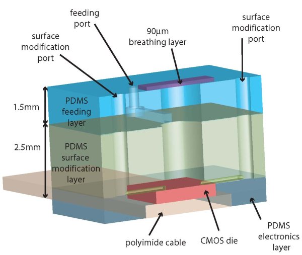
My thesis work focused on developing a hybrid system that combined PDMS microfluidics and CMOS sensing and actuation to create a system for autonomous cell culture and incubator. After defending my thesis, I have continued to make improvements to the system to successfully perform cell culture on par with standard culture.
Cell culture techniques, developed at the turn of the twentieth century, are still, today the fundamental tool in the study of cell function, tissue engineering and pharmacology. Cell culture has revolutionized our understanding of cellular and molecular biology. In addition, cell culture has been integral to the development of mass-production viral vaccines, in vitro fertilization, pharmaceutical screening and toxicology, and it has had a huge impact on public health and quality of life for the vast majority of the world. It is today the cornerstone of biotechnology research. In the past thirty years, some of the greatest advances in biotechnology have been a direct result of basic research based on cell culture techniques such as development of artificial tissue and organs; cultured skins cells are used today as grafts and superior wound dressings in burn victims and skin ulcer patients. Cell culture has also dramatically decreased the need for live-subject testing (both animal and human).
For almost a century traditional cell culture has remained virtually unchanged. Cells are grown in plastic flasks or wells with one experiment each. However, with the development of microfluidics we have moved away from this model to performing many different experiments in a small microfluidic device. Using microfluidics we can change the conditions for each of these experiments and obtain results that previous would have take more time and resources. In addition, soft lithography, the micro-structuring of soft polymer materials, usually poly(dimethylsiloxane), PDMS has drastically improved cell culture (any many other areas of life science research). Soft lithography using PDMS is a low cost (approximately fifty times cheaper than silicon), biocompatibility method of creating devices using techniques that drove the microelectronics revolutions. We now have a simple technique for creating devices for cell culture that, unlike the fabrication of microelectronic devices, requires the use of traditional microfabrication techniques simply to produce a master mold that is reusable almost indefinitely, implying that access to fabrication facilities is not needed in creating the devices, only master copies. This converts per wafer cost both economic and environmental to a per design cost. In fact, an entire journal, Lab on a Chip, is dedicated almost entirely to soft lithography with PDMS.
While there have been many recent developments in microfabricated structures for passive cell culture, in all but one of the published studies a traditional incubator or complex fluidic heating and pumping system is needed for the actual cell culture. There has been only one published paper, that I know of, which attempts to integrate cell culture with "self incubation" in ambient environment. The CBB (cell-based biosensor) reported by Debusschere and Kovacs used an integrated CMOS substrate with PDMS microfluidics for cell culture and biosensing. However, the incubation feature was only used to maintain the cells during biosensing, periods between which the cells were returned to a traditional incubator. Although their system does not eliminate the need for an incubator, the combination of CMOS and incubation is unique and an important milestone.
I have created a new paradigm for microsystem design and fabrication with applications in the life sciences and biotechnology. The essence of the approach is the integration and embedding of CMOS electronics "into" PDMS microfluidics. I have fabricated microsystem that utilizes both disposable microfluidic structure and reusable functional silicon blocks. This is a scalable and cost effective method of integrating basic CMOS integrated circuits with microfluidic structures to control and manipulate liquids and gases. The approach is aimed at simple, inexpensive fabrication methods for components with elementary fluidic functions for use in tandem with very expensive, highly functional components that can be created once for reuse many times in the same or other systems.
As we navigate the "Roadmap for Semiconductors" toward increasingly compact circuits, new technologies have emerged to facilitate growing density. Foremost among these technologies is silicon on insulator (SOI). SOI structures are composed of a thin layer of silicon, usually 50 nm to 100 mm, atop an insulating substrate. However, as feature sizes approached the 10 nm mark, the difficulties and commensurate costs encountered in fabrication has directed interest toward 3D processing. Previously 3D was comparatively so expensive that it was relegated solely to in-house research. With the 10 nm mark on the horizon, 3D has become a viable alternative for increasing circuit density rather than simply attempting to further scale planar devices. This transition, in addition to the combination of 3D and SOI technologies, lead to the first multi-project foundry 3D SOI-CMOS run through MIT-LL which taped out in April, 2005. This 3D SOI-CMOS technology was developed using three SOI-CMOS wafers fabricated in a fully depleted silicon on insulation (FDSOI) process with a single polysilicon layer and three metal layers per wafer or tier.
I fabricated a Self-Biased Operational Transconductance Amplifier in the first run. The description of the amplifier and its characterization have been accepted for publication in the proceedings of ISCAS 2007.
The second run of the 3D SOI-CMOS multi-project foundry run through MIT-LL is underway. I have designed several amplifiers and several CMOS/MEMS structures that were submitted for this run. I am eagerly awaiting the completion of the run to continue work in this area.