Circuit repair using laser activated fuse structures.
Circuit Repair Using Laser Activated Metal Trace Welding
Jovan Trujillo
Flexible Electronics and Displays Center
Arizona State Univerity
10-28-2014
Abstract - In this paper we explore repairing defective thin film circuits using redundant circuitry activated by laser ablation. The test circuit is an active matrix backplane designed with redundant row and column data lines. These extra data lines are isolated from the circuit using cross-over structures insulated with a thin layer of dielectric material. If a data line is defective it is isolated from the circuit using laser cutting and the backup data line is activated by melting the insulated cross-over structure with a laser. A study of the cross-over design and laser pulse parameters has resulted in 96% success in activating data lines. Resistances as low as 1000 Ohms were recorded using this approace.
I. Introduction
Product yield continues to be a major problem in flexible electronics manufacturing. In this paper we cover how a laser cutting system is used for defect isolation. New work will focus on using the laser to re-route circuitry around an isolated defect. This allows for a reduction in the damage of the salvage operation. Entire lines rendered inoperable are reduced to single pixels.
At the FEDC circuit repair currently involves more of a salvage effort than actual repair. An infrared camera is used to identify the locations of excessively high leakage current. For active matrix display prototypes the repair process involves cutting out transistors and crossover structures which show an unreasonably high leakage current. These leakage paths damage the display driver circuitry attached to the array, and therefore damage flexible display prototypes. To control these problems lines are cut out of the array. Line cuts sacrifice the quality of the array for prototype completion. It would be desirable to create a true repair process which can remove leakage paths from an array without destroying entire rows and columns from the display.
II. Experiment
The need for line cutting for leakage reduction leaves unresponsive lines in the active matrix display. For flexible displays in development this can lead to several lines unresponsive in a display.
A. Factorial Design 1
The experiment was set up using a factorial design that tests 8 welding structures. The first 5 structures have a 20 um target area. Structure 1 is a 20 um target composed of a stack of aluminum, dielectric, and molybdenum. Structure 2 is a 20 um target composed of a stack of aluminum, dielectric, an amorphous silicon layer with a via in the center, and molybdenum. Structure 3 is a 20 um target composed of a stack of aluminum, dielectric, amorphous silicon without a hole in the center, and molybdenum. Structure 4 is a 20 um target composed of a stack of aluminum, dielectric, amorphous silicon, molybdenum, ITO, and a via in the center. Structure 5 is a 20 um target composed of a stack of aluminum, dielectric, molybdenum, ITO, and a via in the center. Structure 6 is a 40 um target composed of a stack of aluminum, dielectric, and molybdenum. Structure 7 is a 40 um target composed of a stack of aluminum, dielectric, amorphous silicon with a hole in the center, and molybdenum. Structure 8 is a 40 um target composed of a stack of aluminum, dielectric, amorphous silicon, and molybdenum.
A laser with a wavelength around 510 nm would fire 3 times per fuse. Three power ranges were used at 20%, 50%, and 80% capacity. Two aperture sizes of 10% and 20 % were used. The number of sites fired on a single fuse were either 1 or 4. This created a factorial design of 5 factors with 2,5,3,2,2 levels respectively.
Factorial Design 2
The second factorial design included other laser wavelengths into the study. The factors were 2 laser wavelengths in the gree and IR spectrum, the 8 target structures described in factorial design 1, 3 power ranges at 10%, 25%, and 50%, 2 aperture sizes at 10% and 20%, and 2 flash patterns with 1 site and 4 sites. The laser was changed from 3 shots per site to burst mode with 50 shots per site.
Yield Experiment 1
The results of the factorial analysis indicated that a high laser power would create fuse welds with less than 1 kOhm resistance. The damage created by such a high power blast was theorized to reduce the reliability of the process. Therefore a yield analysis was done with 576 devices to test whether a lower power level would improve the reliability of the process by melting the metal sandwich instead of evaporating the target and welding only along the edges. The experimental conditions for the yield experiements are given in Table 1.
III. Results
A. Factorial Experiment 1
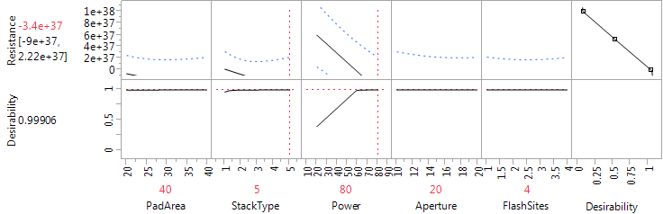
The best conditions derived from the first factorial design showed that the most significant factor is laser power. The best conditions were 40 um target size, a stack structure with a VIA, 80% power, 20% laser aperture size, and 4 sites per target with 3 shots per site.
Fig 1. Results of first factorial design analysis
B. Factorial Experiment 2
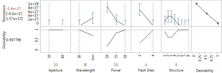
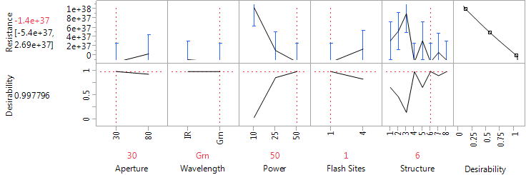
The results of the second experiment again showed that laser power was the most significant factor. The best conditions are given in Table II. The experiment was repeated twice to test for repeatability. The differences between repliates indicated that many of the factors have a weak influence on yield. The results of the experiments are given in Figure 2 and Figure 3.
Fig 2. Results of second factorial design analysis.Fig 3. Results of second factorial desing analysis replicated.
C. Yield Analysis
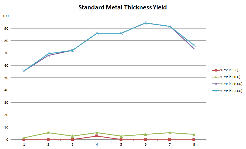
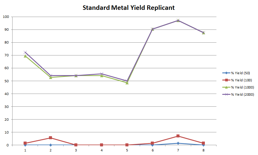
The yield experiment at 50% yield resulted in 23% yield for welds less than 1000 ohms. For the experiment at 25% resulted in 44% yield. As hypothesized the lower energy of the laser evaporated less material. This allowed more material to cover the edges of the ablation zone and increase the possibility of a successful weld. From these results it was further hypothesized that adding more metal to the fuse stack would further increase the probability of a successsful weld.
Fig. 4. Yield of standard metal thicknessFig. 5. Yield of standard metal thicknes replicated
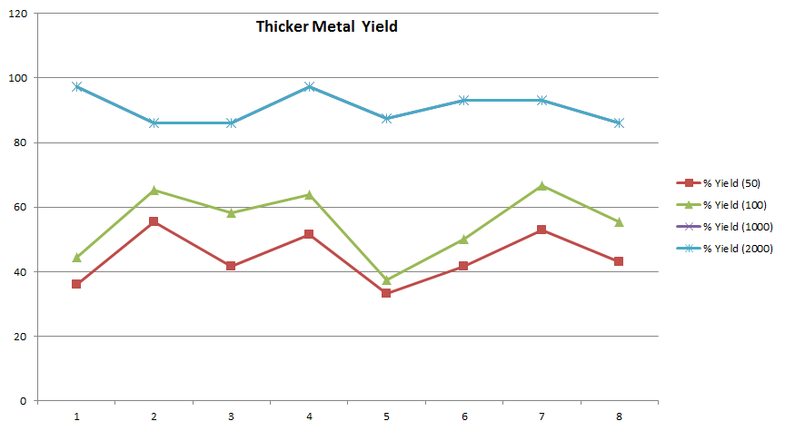
D. Thicker Metal Yield Analysis
The yield was shown to increase with increased metal thicknes. The yield of the standard metal thickness are given in Figures 4 and 5. The yield of the thicker metal stack is given in Figure 6.
Fig. 6. Thicker metal yield experiment
IV. Conclusion
In conclusion the feasability of welding traces in thin film transistor circuits was explored.
50% Power
25% Power
IR Laser
IR Laser
50% Laser Power
25% Laser Power
55% aperture
55% aperture
4 flash sites
4 flash sites
Burst mode
Burst mode
All structures
All structures
Table I. Conditions For First Yield Experiments
Results
30% aperture
IR or green laser
50% laser power
1 or 4 flash sites
structure 6 or 8 (40 $\mu~m$ dielectric stack or 40 $\mu~m$ amorphous silicon stack)
Table II. Best Conditions For Factorial Design 2
References
S.A. Akhmanov, V. I. Emel'yanov, N. I. Koroteev and V. N. Seminogov, Interaction of powerful laser radiation with the surfaces of semiconductors and metals: nonlinear optical effects and nonlinear optical diagnostics, Sov. Phys. Usp. 28(12), December 1985.
Cheng Luo and Liweir Lin, The application of nanosecond-pulsed laser welding technology in MEMS packaging with a shadow mask, Sensors and Actuators A 97-98 (398-404), 2002.
C. P. Grigoropoulos, H. K. Park, and X. Xu, Modeling of pulsed laser irradiation of thin silicon layers, Int. J. Heat Mass Transfer Vol. 36, No. 4, pp. 919-924, 1993.
U. M. Mescheder, M. Alavi, K. Hiltmann, Ch. Lietzau, Ch. nachtigall, H. Sandmaier, Local laser bonding for low temperature budget, Sensors and Actuators A. Vol. 97-98, pp. 422-427, 2002.
Shuichi Torii, Wen-Jei Yang, Heat transfer mechanisms in thin film with laser heat source, International Journal of Heat and Mass Transfer, Vol. 48, pp. 537-544, 2005.
Vasilios Alexiades and David Autrique, Enthalpy Model For Heating. Melting, And Vaporization In Laser Ablation, Electronic Journal of Differential Equations, Conference 19, pp. 1-14, 2010.